
Quality in EMS manufacturing does not come naturally or by chance. Every single employee at A+B Electronic contributes to ensuring and continuously improving quality. PCB assembly is a complex process. Different components, different PCBs, assembly accurate to the millimetre, possibly conformal coating and unit assembly – we have to implement all of this perfectly for our customers so that subsequent value-added processes are not interrupted. Our systematic quality policy is therefore strictly geared to the high requirements of the market for electronic assemblies and devices. In this way, we regularly achieve the lowest error rates.
You want to know more about how we ensure quality? Then you’ve come to the right place.


To protect your personal data, your connection to the video streaming provider has been blocked. Click to unblock the video streaming provider. By loading the video you accept the video streaming provider’s privacy policy. More information about the video streaming provider’s privacy policy can be found here: Google - Privacy & Terms
1. Incoming goods inspection
As soon as we receive the PCBs, we check whether they meet our high requirements. This also applies to supplied stencils in the SMT range. We test components for projects with special requirements individually. We check all components for identity and specification.
2. Initial sample control
With every production order, we check the first assembly produced under series conditions before we continue to have the series produced. In this way, we avoid mass-producing undetected errors and anomalies. We carry out the initial sample inspection with the EFA Inspection® software, among other things.

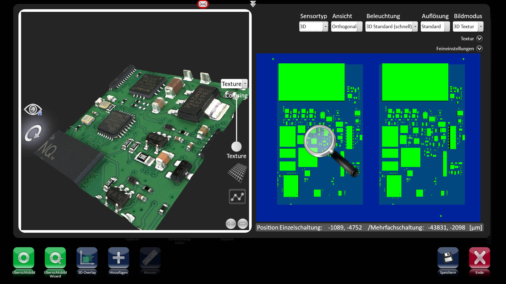
3. X-ray inspection, also Manual X-ray Inspection (MXI)
Some components such as BGAs or QFMs have solder joints on the underside of the component. So we cannot evaluate these solder joints visually without using an X-ray machine. We use X-ray technology to check these components for short circuits, so-called “voids”, offsets or similar defects: The test image is created by the different absorption of the X-rays as they pass through the object. In this way, we make structures visible inside the object that cannot be seen from the outside. We log this inspection if the customer wishes. MXI is becoming increasingly important because it offers decisive advantages. In EMS production, it drastically reduces the overall costs if we detect errors at an early stage. Because this prevents us or our customer from using defective parts in the further value-added steps.

4. Possible intermediate step: SPI
Solder Paste Inspection (SPI) enables fast and accurate inspection of solder paste on printed circuit boards. It checks very time-efficiently whether the paste has been correctly applied to the printed circuit board.
Durch die Due to increasingly complex assembly processes, soldering on modern circuits is much more complicated than it was a few years ago. Due to the introduction of SMT assembly and the miniaturisation of PCBs, soldering is becoming increasingly compact and small-scale. Even average circuit boards have thousands of solder joints. This increasing complexity of PCB assembly also means that comprehensive manual inspection is no longer possible. And even when the manual inspection of each individual PCB was still normal, it quickly became clear that this method was insufficient. The employees tired quickly, their concentration decreased with the number of blanks.
Since our customers and our customers’ customers today demand high quantities at the highest possible speed, reliable and fast methods of quality assurance are required. The SPI is a major breakthrough in this respect and inserts itself into the production line directly after the solder printing process. In this way, we detect problems in the production process at an early stage.
5. AOI in 2D and 3D after SMD assembly
Automated optical inspection (AOI) is a typical inspection step in the assembly of PCBs. AOI uses a camera system that independently inspects the component at different levels:
- Check for missing components
- Testing for component displacement
- Inspection of the pilot stations
- Check for twisting / polarity reversal
AOI is a non-contact inspection method that we can use at many stages of the manufacturing process. Examples are the inspection of assembled PCBs or post-reflow inspection. However, the typical time of use for AOI systems comes after solder reflow. These so-called post-reflow AOI systems check for most types of defects (component placement, solder short circuits, missing solder).
Advantage of the post-reflow inspection: The inspection happens at a point in the line where the entire board can be inspected with a single system. We can rework faulty blanks and send the other blanks to the next process stage. We store data from the AOI check for future applications. The evaluation of the AOI error formation by a specialist is called manual optical inspection.
If, after this step, the assembly assembled by the SMD revision passes to the THT area, we carry out another initial sample inspection there.
6. THT revision
If we solder components onto the assembly using through-hole technology, there is a separate step for quality assurance. In the THT revision, we check the entire soldering of the THT components.
“There are very many opportunities in our industry for the smallest deviations to cause defects immediately. We can only counter this through meticulous testing.”
Klaus Martens
Technical Quality Assurance
7. Final inspection
The final inspection is a final visual inspection of the finished PCBs. Here, it’s about everything from the overall impression to the details: How does the board look when the customer unpacks it, are all the stickers firmly in place, has the Conformal Coating Department worked perfectly and cleanly?
8. Outgoing goods inspection
Depending on the requirements and the customer, we visually check the finished blanks again here. We do this at least on a random basis, but in certain cases also 100%. This is like a second final inspection directly in the goods issue area, so that a 4-eyes principle once again minimises the error rate.
In addition to our usual quality assurance measures, we also offer special testing and inspection procedures for individual industries and special requirements of our customers. Do you have questions about this or do you need an EMS service provider? Then we look forward to receiving your enquiry.
Do you need a company that offers more than just assembly?
Then find out more about us here – or contact us directly without obligation. Then we talk about future projects and how we can grow together.


